Interfacing AT93C46 SPI EEPROM with avrPrayog
About Serial Peripheral Interface aka SPI
- Serial peripheral Interface or SPI is one of the standard communication protocol between two chips (ICs).
- Sometimes some datasheets name it as 3 wire interface, Basically this protocol uses 4 wires or lines to make it complete.
- Its a Master, Slave type scheme that means out of two communicating ICs, one acts as Master and Other one as Slave.
- Its a Synchronous protocol all data transfer is synchronized through a clock.
- total 4 wires are used MOSI, MISO, SCK, CS. CS is not always used, it may be tied permanently to appropriate value.
- MOSI → Master Out Slave In (Data from Master to Slave travels this wire)
- MISO → Master In Slave Out (Data from Slave to Master travels on this wire)
- SCK → Serial Clock (Serial Clock signal generated by Master)
- CS → Chip Select (it may be used in multiple slaves case to select a particular slave )
SPI communication is based on MASTER, SLAVE concept. One of the communicating device is master and other is slave. SPI can be viewed as an Synchronous 16 bit[1] shift register with an 8 bit half residing in the Master side and other 8 bit half residing in the Slave side. Simply speaking it makes a common 16 bit circular buffer shared between master and slave. The basic concept is that, when master pulse out a bit of data, immediately it comes in the shift register of slave. everything is synchronized with the master clock generated by Master device.
Master can select one of many slaves by pulling Slave Select pin (SS)of that particular device LOW. When slave's pin (SS)is made low by Master, slave's shifting capability is enabled.
Master pulse out data bits on MOSI (Master Out Slave In) line, Slave pulse out data bits on MISO (Master In Slave Out) synchronized with the clock generated by Master.After eight master clock pulses on SCK line, a byte of data has been exchanged between master and slave designated SPI devices. Completion of data transmission by Master and reception by slave is signaled by setting of SPIF flag by SPI module. SPIF flag bit is located as the 7th bit (MSB) of SPSR (SPI status register).
AT93C46
AT93C46 is an interesting chip. Its a non volatile memory or EEPROM, giving you just 1024 bits of electrically erasable programmable read only memory. It can be used as 128×8 bits fashion or 64×16 fashion, depending on logic level at ORG pin of 93c46.
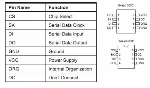 When the ORG pin is connected to Vcc, 16×64 fashion is chosen and when ORG is connected to GROUND 8×128 fashion is chosen. There are a few commands that are needed to perform specific memory operations like ERASE, READ, WRITE etc. below is a table showing All the available commands for at93c46.
- There are a few tricks that you need to know in order to interface at93c46 to any controller. Although the memory is arranged in either 16 bit fashion or 8 bit fashion but the commands that you need to send to at93c46 is not always multiple of 8. So you need to carefully pack the Start bit, Op Code , Address and data information in multiple of 8 if you are going to use standard (you find in AVR, PIC) SPI module, which allows 8 bit data transmission at any time.
- Lets try to understand by an example, Suppose you want to erase send the ERASE command to 93c46. according to the table of instructions given in Datasheet. The instruction looks like this.

- How will you send total 10 bits (1 Start Bit, 2 Op Code bits, 7 Address bits) using a register SPDR which is 8 bits wide. Naturally you need to send it in 2 times in continuation. So how are we going to fit the 10 bit data into 16 bit wide packet. Let me show you how !
Everything about AT93C46 is fine, and easy to implement using standard SPI module provided in AVR Microcontrollers. BUT, there is one problem, I don't know why designer of AT93C46 made it that way. According to datasheet of AT93C46, while pushing out data on DO line it inserts an initial ZERO before 8 bit or 16 bit data comes out. That means every data you receive from AT93C46, a ZERO will precede all communication from Memory to controller. This is a huge drawback as i see it, it makes this easy to use IC a little difficult one. Because when using standard SPI module such as in AVR. It is not possible to skip just one bit deliberately. It may be easy when you are generating clock in software, in that case you can strobe one clock pulse to skip the initial ZERO bit. So, overall if you thought interfacing AT93C46 with AVR is simple, its not that simple.
Things Required
| Serial | Part name | Image |
|---|---|---|
| 1 | 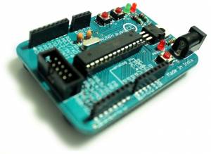 | avrPrayog board with ATmega328 running at 16MHz |
| 2 | 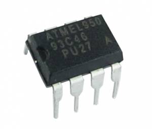 | at93c46 SPI EEPROM chip costs around Re 10 Only |
| 3 |  | Solder less Breadboard |
| 4 | Some Jumper Wires |
 // main.c created for project at93c46 on 09/18/2012 11:06:14

 /*****************************************
 Devesh Samaiya
 devesh@electroons.com
 ******************************************/

 #include<avr/io.h>
 #include<util/delay.h>
 #include "spi.h"
 #include "defs.h"
 #include "lcd.h"


 int EWEN()
 {
       SPI_PORT &=~(1<<SS);
       SPI_PORT |= (1<<SS);
       master_transmit(0x02);
       master_transmit(0x60);
       SPI_PORT &=~(1<<SS);
       _delay_ms(10);
       return TRUE;
 }

 int AT93C46_EraseAll()
 {
       SPI_PORT &=~(1<<SS);
       SPI_PORT |= (1<<SS);
       master_transmit(0x02);
       master_transmit(0x40);
       SPI_PORT &=~(1<<SS);
       SPI_PORT |= (1<<SS);
       while(!(SPI_PIN & 1<<MISO)); // Wait till memory is Busy
       SPI_PORT &=~(1<<SS);
       return TRUE;
 }

 int AT93C46_ERASE(unsigned char address)
 {
       SPI_PORT &=~(1<<SS);
       SPI_PORT |= (1<<SS);
       master_transmit(0x03);
       master_transmit(0x80|address);
       SPI_PORT &=~(1<<SS);
       SPI_PORT |= (1<<SS);
       while(!(SPI_PIN & 1<<MISO)); // Wait till memory is Busy
       SPI_PORT &=~(1<<SS);
       return TRUE;
 }

 int AT93C46_WR(unsigned char address, unsigned char data)
 {
       SPI_PORT &=~(1<<SS);
       SPI_PORT |= (1<<SS);
       EWEN();
       SPI_PORT &=~(1<<SS);
       SPI_PORT |= (1<<SS);
       master_transmit(0x02);
       master_transmit(0x80|address);
       master_transmit(data);
       SPI_PORT &=~(1<<SS);
       SPI_PORT |= (1<<SS);
       while(!(SPI_PIN & 1<<MISO)); // Wait till memory is Busy
       SPI_PORT &=~(1<<SS);
       _delay_ms(10);
       return TRUE;
 }

 unsigned char AT93C46_RD(unsigned address)
 {
       unsigned char read;
       SPI_PORT &=~(1<<SS);
       SPI_PORT |= (1<<SS);
       master_transmit(0x03);
       master_transmit(address);
       _delay_ms(10);
       read = master_transmit(0x00); //dummy write to collect data
       SPI_PORT &=~(1<<SS);
       return read;
 }

 // To store a string starting at address
 int AT93C46_WR_STR(unsigned char address, unsigned char *data)
 {
       int count;

       for(count=0;data[count]!='\0';count++)
       {
               AT93C46_WR((address+count),data[count]);
       }
       return TRUE;
 }

 unsigned char* AT93C46_RD_STR(unsigned char address)
 {
       int count;
       unsigned char *ret,data;

       for(count=0;;count++)
       {
               data=AT93C46_RD(address+count);
               if(data=='\0')
               break;
               else
               ret[count]=data<<1;

       }

       return ret;
 }


 int main(void)
 {
       unsigned char data,data1;
       lcd_init(LCD_DISP_ON);
         lcd_clrscr();

       SPI_DDR |= 1<<MOSI | 1<<SCK | 1<<SS;
       SPI_DDR &= ~(1<<MISO);


       master_init();

       if(!EWEN())
       error("EWEN");


       if(!AT93C46_EraseAll())
       error("ERAL Fail");


         if(!AT93C46_WR(0x20,'D'))
       error("Write Fail");

         if(!AT93C46_WR(0x02,'Z'))
       error("Write Fail");

       data = AT93C46_RD(0x20);
       lcd_gotoxy(0,1);
       lcd_putc(data<<1);

       data1 = AT93C46_RD(0x02);
       lcd_gotoxy(1,1);
       lcd_putc(data1<<1);


       while(1);

       return 0;
 }
- – devesh@electroons.com 2012/09/21 15:09 no copyrights: you have all rights to copy