
Basics of GPIO in LPC21xx - ARM7 Tutorials
— January 28, 2013Basic Registers
Download User Manual for LPC2148 Chapter 7, PAGE 75
PINSEL Registers
Most of the pins on LPC2148 are multifunctional, every pin can be used to perform one of the assigned function to it depend on the setting of PINSEL register of the specific port to which that pin belongs.
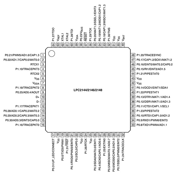
For example in the LPC214X pin diagram above, pin number 1 is labeled as “P0.21/PWM5/AD1.6/CAP1.3″ , it means this pin can function in 4 modes. It can be either…
- PORT0.21 (GPIO) or
- PWM Out 5 or
- ADC 1 input for channel 6 that is AD1.6 or
- CAP1.3 Timer Capture Pin
Out of the listed 4 possible functions, Pin 1 can function as any one at once. Current function of any pin can be configured using corresponding PINSEL register in this case PINSEL0 or PINSEL1 (have to check in datasheet), for every multi-functional pin, default functionality is always GPIO provided GPIO is one of the functions.
for LPC2148 there are 3 PINSEL registers, PINSELx (x : 0,1,2), refer to datasheet for more details check table 60 onwards.
GPIO Registers
Fast GPIO Registers
To enable Fast Input Output, System Control and Status register (SCS) should be given value 3.
REFER to User Manual for more details on IODIR, IOSET, IOCLR check on Page number 81 onwards, its Chapter 8
For writing C Code recipe…
IO0DIR = 0×00000080; // Pin PORT0.7 configured as output
IO0SET = 0×00000080; //Pin PORT0.7 goes HIGH
IO0CLR = 0×00000080; //Pin PORT0.7 goes LOW
IO0SET = 0×00000080; //Pin PORT0.7 goes HIGH
Difference between FAST & GP Input Output
I hope you can intuitively deduce the difference between Fast GPIO and Generel Purpose Input Output. Fast input output controller block is connected to the ARM local bus while GPIO block is connected with Peripheral Bus of the controller system.
A note about usage of IOPIN register…
Write to the IOPIN register enables instantaneous output of a desired content on the parallel GPIO. Binary data written into the IOPIN register will affect all output configured pins of that parallel port: 0s in the IOPIN will produce low level pin outputs and 1s in IOPIN will produce high level pin outputs. In order to change output of only a group of PORTA pins, application must logically AND readout from the IOPIN with mask containing 0s in bits corresponding to pins that will be changed, and 1s for all others. Finally, this result has to be logically ORred with the desired content and stored back into the IOPIN register.
For Example-
IO0PIN = (IO0PIN && 0xFFFF00FF) | 0x0000A500
About author


Leave a reply